Emulation of Fujitsu MB8877 Floppy Disk Controler with Arduino
Context
I have a Yamaha QX1 MIDI sequencer from 1984.
I want to replace the floppy drive (Canon MF-221) and the Floppy Disk Controler (Fujitsu MB8877a) with an Arduino.
The project
Description
The Fujitsu MB8877 is a second source for Western Digital FD1793.
(white pins are not connected on the QX1 DM board)

| Pin | Name | Function | Driven by | Description |
|---|---|---|---|---|
| 37 | /DDEN | Double Density | QX1 | Permanently ↓ as we only use Double Density disks (256 bytes/sector) |
| 3 | /CS | Chip Select | QX1 | Permanently ↓ (always selected) |
| 24 | CLK | Clock | QX1 | Times the FDC logic; we don't use this signal to clock the Arduino. However, the clock starts only ~5.4 msec after powering up the QX1; before that, all signals are garbage. |
| 19 | /MR | Master Reset | QX1 | Used during boot. MR ↓ ~4.6 msec after power up (the main CPU Hitachi HD68B09 only needs 110 nsec @ 8 MHz to boot). |
| 7 to 14 | DAL0-7 | Data bus | both | This bus is shared by several ICs on the board:
|
| 5 | A0 | Address 0 | QX1 | Selects register (cf table below) |
| 6 | A1 | Address 1 | QX1 | |
| 2 | /WE | Write Enable | QX1 | selects function (cf table below) |
| 4 | /RE | Read Enable | QX1 | |
| 39 | IRQ | Interrupt Request | FDC | Goes ↑ to warn the QX1 the previous command is completed |
| 38 | DRQ | Data Request | FDC | Goes ↑ to warn the QX1 data is available (read) or is required (write) on DAL0-7. |
| 17(*) | Early | FDC | Pre-compensation signals. These signals are used to shift the timing of data to be written on the disk. 0=No pre-comp, 1=Pre-comp. | |
| 18(*) | Late | FDC | ||
| 29(*) | TG43 | Track > 43 | FDC | Warns the CPU on head position. 0=head on track 0 to 43, 1=head on track 44 to 76. |
| 31(*) | WD | Write Data | FDC | Data to be written on the disk drive |
 The protocol

The protocol between the MPU and the FDC is driven by the MPU. It basically consists for the MPU to read or post data in the FDC's registers. To do so, the MPU controls 5 pins: /CS (to select the FDC), /RE and /WE (to select read or write), A1 and A0 (to select the register).
As mentioned earlier, /CS is grounded: the chip is always selected.
Thus, the control is ensured by 4 pins, summarized in this table:
| /CS | A1 | A0 | /RE | /WE |
Function
|
|---|---|---|---|---|---|
| 0 | 0 | 0 | 0 | 1 |
MPU wants to read Status Register
|
| 0 | 0 | 1 | 0 | 1 |
MPU wants to read Track Register
|
| 0 | 1 | 0 | 0 | 1 |
MPU wants to read Sector Register
|
| 0 | 1 | 1 | 0 | 1 |
MPU wants to read Data Register
|
| 0 | 0 | 0 | 1 | 0 |
MPU wants to write into Command Register
|
| 0 | 0 | 1 | 1 | 0 |
MPU wants to write into Track Register
|
| 0 | 1 | 0 | 1 | 0 | MPU wants to write into Sector Register |
| 0 | 1 | 1 | 1 | 0 |
MPU wants to write into Data Register
|
| 0 | - | - | 0 | 0 |
Not specified in the datasheet: see below
|
The situation where both /WE (MPU want to read a register) and /RE (MPU wants to post to a register) are low simultaneously is not specified in the datasheet, and doesn't make sense. However, I measured a lot of cases where both /WE and /RE are down.
Schematic
The schematic can be found here: Project schematic (PDF)Some explanations
U1 (74LS245): buffer with DAL0-7U3 (74LS244): buffer from the keyboard and the command pins (A0, A1, /RE and /WE)
U3 (74LS244): buffer to the LCD
U7 (74HC125): voltage adaptor (5V -> 3.3V) for the SD card and reverse voltage for the keyboard.
U4A (74LS139): this component manage the 8 bit bus (port D on the Arduino) by enabling/disabling the buffers U1, U3 and U6. U4A is managed via port C with the following table:
| C3 | C2 | C1 | C0 | D7 | D6 | D5 | D4 | D3 | D2 | D1 | D0 | Sens | Description |
|---|---|---|---|---|---|---|---|---|---|---|---|---|---|
| 1 | - | - | - | - | - | - | - | - | - | - | - | - | High Z |
| 0 | - | 1 | 1 | DB7 | DB6 | DB5 | DB4 | - | R/W | E | - | Output | LCD |
| 0 | - | 1 | 0 | << | < | > | >> | - | - | - | - | Input | Keyboard |
| 0 | - | 0 | 1 | - | - | A1 | A0 | /WE | /RE | - | - | Input | Command |
| 0 | 0 | 0 | 0 | DAL7 | DAL6 | DAL5 | DAL4 | DAL3 | DAL2 | DAL1 | DAL0 | Input | Data |
| 0 | 1 | 0 | 0 | DAL7 | DAL6 | DAL5 | DAL4 | DAL3 | DAL2 | DAL1 | DAL0 | Output | Data |
The QX1 - timings
All the timings below are measured with a Saleae Logic 8 Analyzer at 12 Ms/Sec.Bootup sequence
Here are the chronograms (timing) of the QX1 bootup sequence.


Problem with /RE and /WE
On the MB8877 datasheet, no information if both are low. However, I found many situation where /RE and /WE are both down.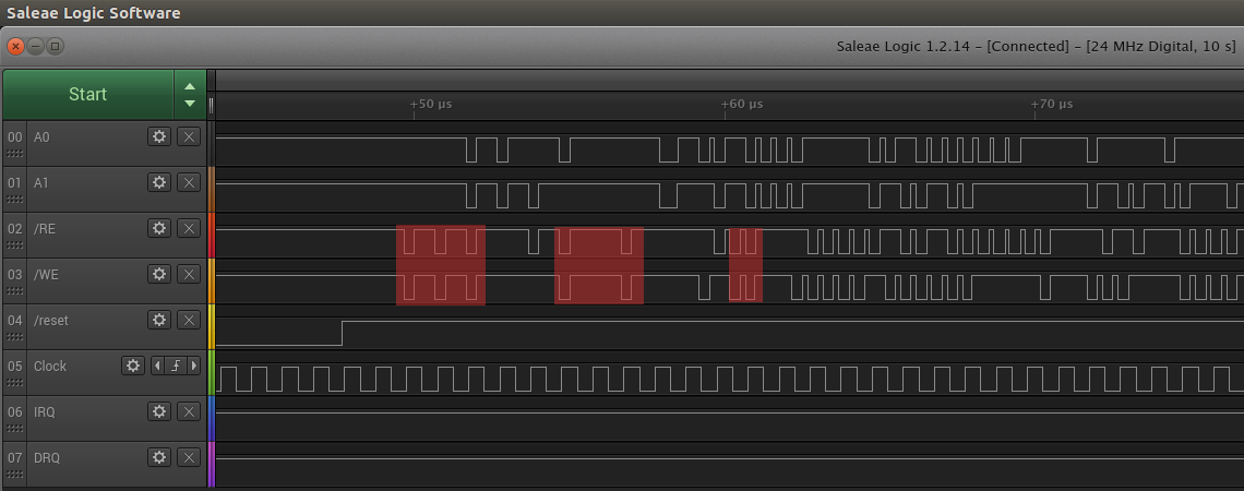 |
| Examples where /RE and /WE are both low, an undefined situation. |
Timing for the read operation
The timing for a read operation (the MPU wants to read a register of the FDC) is the following:


Update
My logic analyzer was only 8 channels, not enough to capture the protocol. I purchased a 16 channels analyzer and made new captures. Here are the results:Capture 0: initialization. The trigger is set on /MR ↗, we can clearly see the protocol starting.


Comments